4.5. Memory
4.5.1. Memory Addressing
The instruction set shall use 16-bit logical addresses to provide for referencing of 65,536 words. When the expanded memory option (see Section 4.5.2) is not implemented, physical addresses shall equal logical addresses.
4.5.1.1. Memory Addressing Arithmetic
Arithmetic performed on memory logical addresses shall be modulo 65,536 such that references to the maximum logical address of FFFF16 plus 1 shall be to logical address 000016.
4.5.1.2. Memory Addressing Boundary Constraints
There shall be no odd or even memory address boundary constraints.
4.5.2. Expanded Memory Addressing (optional)
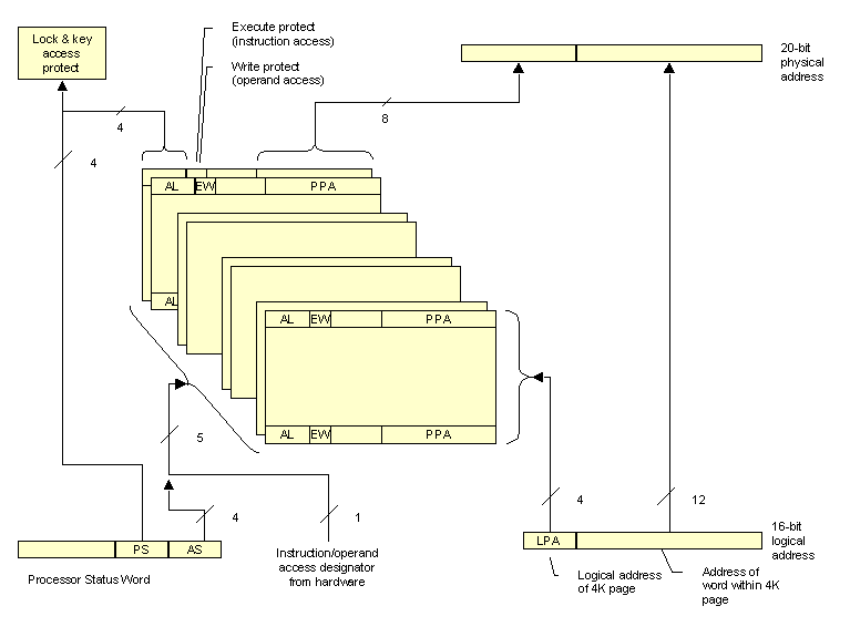
If used, then expanded memory addressing shall be performed via a memory paging scheme as depicted in Figure 1. There shall be a maximum of 512 page registers in the page file (not in logical memory space). These shall functionally be partitioned into 16 groups with 2 sets per group and 16 page registers per set. Within a group, one set shall be designated for instruction references and the other set for operand references. The page size shall be 4096 words such that one set of 16 page registers shall be capable of mapping 65,536 words defined by a 16-bit logical address. The page group shall be selected by the 4-bit Address State (AS) field of the Status Word (SW). The instruction/operand set within the group shall be selected by the hardware that differentiates between instruction and operand memory references. The 4 most significant bits of any 16-bit logical address shall select the page register within that set. The 8-bit Physical Page Address (PPA) within the page register shall be concatenated with the 12 least significant bits of the logical address to form a 20-bit physical address, allowing addressing of 1,048,576 words of physical memory. If expanded memory addressing is implemented, then devices other than the CPU which access memory may utilize either an unmapped 20-bit physical address or a mapped 16-bit logical address. If the devices other than the CPU which access memory utilize 16-bit addressing, a separate address state value must be provided.
4.5.2.1. Group Selection
During instruction and operand references to memory, the address state (AS) field of the status word shall be used to designate the page file group. During an interrupt recognition sequence, the operand set of group zero shall be used for vector table and service pointer references to memory; while the linkage pointer references to memory shall use the operand set specified by the AS of the new status word. During memory accesses by devices other than the CPU which utilize 16-bit logical addressing, the address state value provided by the device shall be used to designate the page register group. Device accesses shall utilize the operand set of the selected group.
4.5.2.2. Page Register Word Format
Each page register shall be 16 bits. The figure below indicates the format for the page register words with the following paragraphs describing the meaning of the access lock (AL) field, the execute protect (E) bit, the write protect (W) bit, reserved bits, and the Physical Page Address (PPA) field.
-----------------------------------------
|   AL   |EW| Reserved |       PPA      |
-----------------------------------------
  0     3  4  5       7  8            15
- AL Field:
-
The access lock and key feature is optional if expanded memory addressing is implemented. If the access lock and key feature is not implemented, then the AL field shall always be zero. If it is implemented, then a 4-bit field (bits 0 through 3) of each page register shall contain the access lock (AL) code for the associated page register, which shall be used with the access key codes to determine access permission. If the access lock and key feature is implemented, the access key code is normally supplied by the PS field of the status word. However, during memory accesses by devices other than a CPU which utilize 16-bit logical addressing, the access code must be supplied by the device.
For each of the possible 16 values of the AL code, access shall be permitted for the reference according to Table VII. References supplying an unacceptable access key code shall not modify any memory location or general registers and an access fault shall be generated. An access fault resulting from a CPU reference attempt shall set fault register bit 0 to cause a machine error interrupt. An access fault resulting from a DMA attempt shall set fault register bit 1 to cause a machine error interrupt. Note that the access lock and key codes defined in the above table have the following characteristics:
-
An access lock code of F16 is an "unlocked" lock code and allows any and all access key codes to be acceptable.
-
An access key code of 0 is a "master" key code and is acceptable to any and all access lock codes.
-
Access key codes 1 through E16 are acceptable to only their own "matched" lock code or the "unlocked" lock code of F16.
-
An access key code of F16 is acceptable to only the "unlocked" lock code of F16.
-
- E Bit:
-
For instruction page register sets only, bit 4 shall be defined as the E bit and shall determine the acceptable/unacceptable criteria for read references for instruction fetches. When E=1, any attempted instruction read reference designating that associated page register shall be terminated and an execute protect fault shall be generated. An execute protect fault shall set fault register bit 0 to cause a machine error interrupt.
- W Bit:
-
For operand page registers only, bit 4 shall be defined as the W bit and shall determine the acceptable/unacceptable criteria for write references. When W=1, any attempted write reference designating that associated page register shall not modify any memory location and a write protect fault shall be generated. A write protect fault resulting from a CPU reference attempt shall set fault register bit 0 to cause a machine error interrupt. A write protect fault resulting from a DMA reference attempt shall set fault register bit 1 to cause a machine error interrupt.
- Reserved Bits:
-
Bits 5 through 7 of all the page registers shall be reserved and shall always be 0.
- PPA Field:
-
An eight-bit field (bits 8 through 15) of each page register shall be dedicated to the physical page address which is used to define the physical address as depicted in Figure 1.
4.5.2.3. Partial Implementations of Expanded Memory Addressing
A given implementation of this standard may include a partial implementation of the expanded addressing option. That partial implementation may use 2, 4, or 8 groups of page registers as follows:
Within any full or partial implementation, the lock feature may or may not be included.
4.5.3. Memory Parity (optional)
If used, then bit 2 in the fault register shall be set to indicate a memory parity error.
4.5.4. Memory Block Protect (optional)
If used, shall be as described by the input/output instructions. For operations which contain multiple memory references, each store operation shall be as defined by the memory protection for that specific memory address.
4.5.5. References to Unimplemented Memory
Attempted access to physical addresses which are not implemented shall generate an illegal address fault and shall cause the referencing action to terminate. An illegal address fault shall set fault register bit 8 to cause a machine error interrupt.
4.5.6. Start up ROM (optional)
If used, the start up read only memory (ROM) address range shall be contiguous starting from physical address 0 up to a maximum of 65,536, as required by the system application. When the start up ROM is enabled, if an I/O or CPU store function is executed whose address is within the start up ROM, then the store is attempted into the main memory. When the start up ROM is enabled, if a read function (instruction or operand) is executed from either I/O or the CPU whose address is to the start up ROM, then the read shall be from the start up ROM. When disabled, the start up ROM cannot be accessed.
4.5.7. Reserved Memory Locations
Locations 2 through 1F16 are reserved. Locations 2016 through 3F16 are used by the hardware and the stored program as defined by Table VIII.